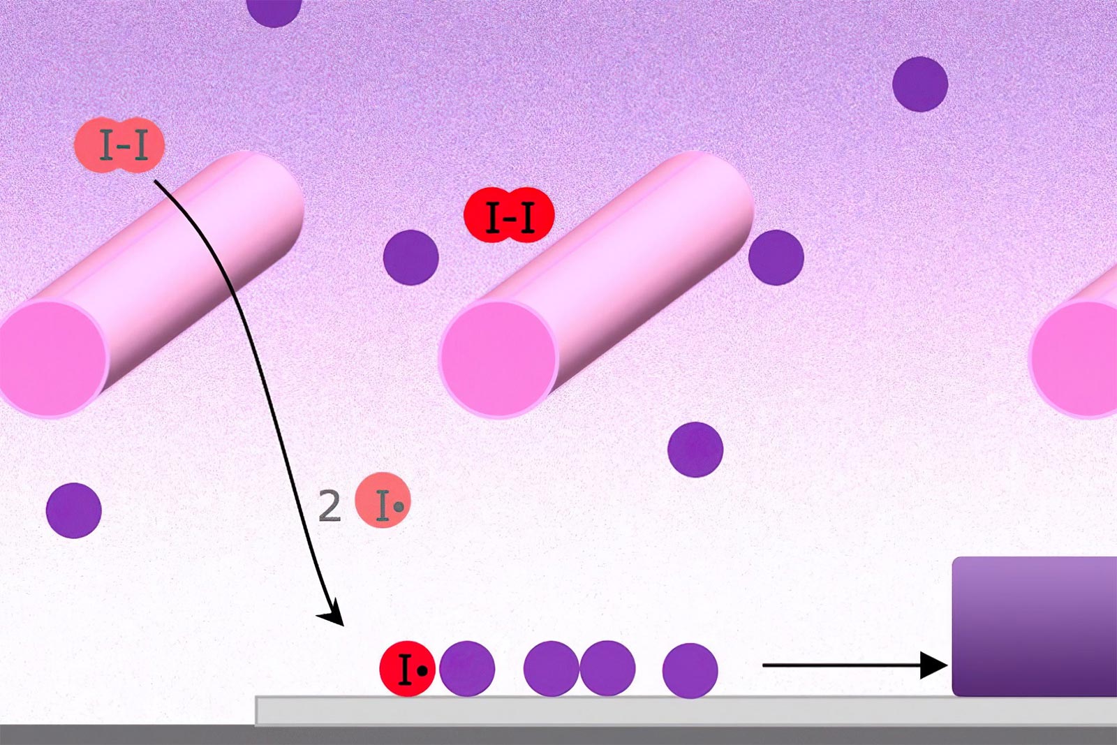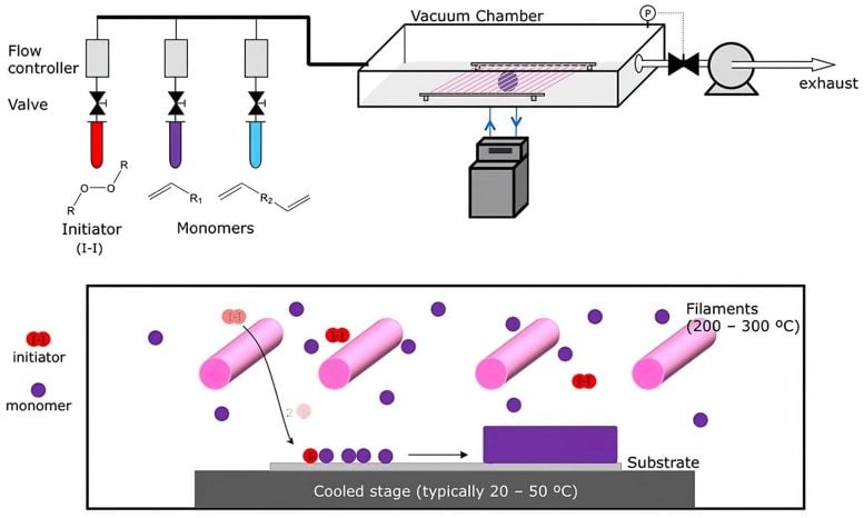
In the process called initiated chemical vapor deposition (iCVD), Heated wires (pink cylinders) cause “initiator” molecules (red) to split, and they then interact with the monomers (purple) used for coating, causing them to collect on the cooler surface below, where they react to form a polymer chain as they build up in a uniform coating (bottom right). Credit: Illustration courtesy of Karen Gleason
Technique enables production of pure, uniform coatings of metals or polymers, even on contoured surfaces.
MIT’s Karen Gleason has advanced Chemical Vapor Deposition (CVD) techniques, transforming it from a high-temperature to a low-temperature process, enabling the deposition of delicate materials like organic polymers. Her work has broadened the applications of CVD, allowing the creation of uniform coatings of metals or polymers on various surfaces. Gleason’s innovation also led to the production of materials from insoluble precursors and the formation of stronger bonds between coatings and substrates. Further evolution of CVD includes high-temperature applications like creating graphene sheets and carbon nanotube arrays.
In a sense, says MIT chemical engineering professor Karen Gleason, you can trace the technology of chemical vapor deposition, or CVD, all the way back to prehistory: “When the cavemen lit a lamp and soot was deposited on the wall of a cave,” she says, that was a rudimentary form of CVD.
Today, CVD is a basic tool of manufacturing — used in everything from sunglasses to potato-chip bags — and is fundamental to the production of much of today’s electronics. It is also a technique subject to constant refining and expansion, pushing materials research in new directions — such as the production of large-scale sheets of graphene, or the development of solar cells that could be “printed” onto a sheet of paper or plastic.
In that latter area, Gleason, who also serves as MIT’s associate provost, has been a pioneer. She developed what had traditionally been a high-temperature process used to deposit metals under industrial conditions into a low-temperature process that could be used for more delicate materials, such as organic polymers. That development, a refinement of a method invented in the 1950s by Union Carbide to produce protective polymer coatings, is what enabled, for example, the printable solar cells that Gleason and others have developed.

The CVD process begins with tanks containing an initiator material (red) and one or more monomers (purple and blue), which are the building blocks of the desired polymer coating. These are vaporized, either by heating them or reducing the pressure, and are then introduced into a vacuum chamber containing the material to be coated. The initiator helps to speed up the process in which the monomers link up in chains to form polymers on the surface of the substrate material.
Credit: Illustration courtesy of Karen Gleason
This vapor deposition of polymers has opened the door to a variety of materials that would be difficult, and in some cases impossible, to produce in any other way. For example, many useful polymers, such as water-shedding materials to protect industrial components or biological implants, are made from precursors that are not soluble, and thus could not be produced using conventional solution-based methods. In addition, says Gleason, the Alexander and I. Michael Kasser Professor at MIT, the CVD process itself induces chemical reactions between coatings and substrates that can strongly bond the material to the surface.
Gleason’s work on polymer-based CVD began in the 1990s, when she did experiments with Teflon, a compound of chlorine and fluorine. That work led to a now-burgeoning field detailed in a new book Gleason edited, titled “CVD Polymers: Fabrication of Organic Surfaces and Devices” (Wiley, 2015).
At the time, the thinking was that the only way to make CVD work with polymer materials was by using plasma — an electrically charged gas — to initiate the reaction. Gleason tried to carry out experiments to prove this, beginning by running a control experiment without the plasma in order to demonstrate how important it was for making the process work. Instead, her control experiment worked just fine with no plasma at all, proving that for many polymers this step was not necessary.
But the equipment Gleason used allowed the temperature of the gas to be controlled separately from that of the substrate; having the substrate cooler turned out to be key. She went on to demonstrate the plasma-free process with more than 70 different polymers, opening up a whole new field of research.
The process can require a lot of fine-tuning, but is fundamentally a simple set of steps: The material to be coated is placed inside a vacuum chamber — which dictates the maximum size of objects that can be coated. Then, the coating material is heated, or the pressure around it is reduced until the material vaporizes, either inside the vacuum chamber or in an adjacent area from which the vapor can be introduced. There, the suspended material begins to settle onto the substrate material and form a uniform coating. Adjusting the temperature and duration of the process makes it possible to control the thickness of the coating.
With metals or metal compounds, such as those used in the semiconductor industry, or the silvery coatings inside snack bags, the heated metal vapor deposits on a cooler substrate. In the polymer process, it’s a bit more complex: Two or more different precursor compounds, called monomers, are introduced into the chamber, where they react to form polymers as they deposit on the surface.
Even high-temperature CVD processing has evolved, with great potential for commercial applications. For example, the research group of John Hart, an associate professor of mechanical engineering, has built a roll-to-roll processing system using CVD to make sheets of graphene, a material with potential applications ranging from large-screen displays to water-filtration systems. Hart’s group and others have used CVD to produce large arrays of carbon nanotubes, materials with potential as new electrodes for batteries or fuel cells.
“It’s a very versatile and widely used manufacturing process,” Hart says, “and a very general process that can be tailored to many different applications.”
One great advantage of CVD processing is that it can create coatings of uniform thickness even over complex shapes. For example, CVD can be used to uniformly coat carbon nanotubes — tiny cylinders of pure carbon that are far more slender than a hair — such as to modify their mechanical properties and make them react chemically to certain substances.
“By combining two CVD processes — one to grow the carbon nanotubes, and another to coat the nanotubes — we have a scalable way to manufacture nanomaterials with new properties,” Hart says.
Much progress in CVD research in recent years traces back to Gleason’s unexpected discovery, back in the 1990s, that the process could work without plasma — and her follow-up on that finding. “You need to pay attention when a new thing happens,” she says. “That’s sort of the key.”
Adblock test (Why?)
Chemical Vapor Deposition (CVD) Explained - SciTechDaily
Read More

